


Contents
Share
Researchers have overcome a major technical challenge to creating organic multifunctional devices that both light up and power themselves
Organic semiconductors are useful materials for both electronic displays and solar cells, but combining efficient light emission and power generation in a single device has been difficult. In a recent study, researchers from Japan addressed this challenge by precisely tuning energy states at the interface of advanced optoelectronic materials. Their approach enables high-efficiency operation and full-color emission, paving the way for multifunctional devices that can both produce and harvest light.
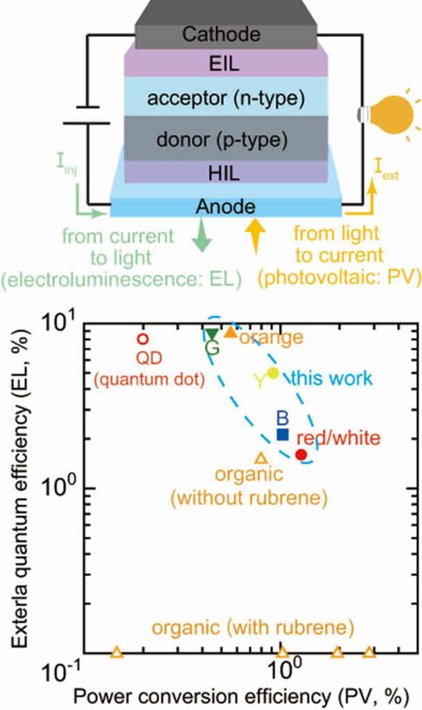
Image title: Design and performance of the proposed multifunctional device
Image caption: The top image is a schematic of a multifunctional device, with the directions of charge flow specified for the electroluminescence and photovoltaic functionalities. The bottom chart depicts a comparison of multifunctional devices in terms of power conversion efficiency and external quantum efficiency for electroluminescence (light generation).
Image credit: Professor Hirohiko Fukagawa from Chiba University, Japan
Source link: N/A
Image license: Original content
Usage Restrictions: Credit must be given to the creator.
Organic semiconductors are thin, flexible, and extremely versatile materials that have revolutionized the world of consumer electronics. They are the core technology behind organic light-emitting diode (OLED) displays, which deliver the vivid colors and contrast seen in modern smartphones and televisions. Additionally, there are ongoing research efforts to harness these same materials for organic photovoltaics (OPVs), aiming to create flexible and cost-effective solar cells that could be embedded into our living spaces and devices. For many scientists, the ultimate goal of this field would be to combine these two functions—light emission and energy harvesting—into a single multifunctional component.
However, this vision has been hindered by a seemingly fundamental efficiency trade-off. Devices that combine both functions must leverage delicate processes involving excitons, which are bound states involving an electron and a positively charged hole (an electron vacancy). For light-emitting functionality, one needs excitons to tightly recombine to create light. Conversely, for power-generating functionality, one needs excitons to quickly dissociate into free electric charges that can be collected elsewhere. This results in a trade-off that has hindered the development of a single component, comprising both functionalities. Designing a single component that can efficiently perform both at the same time has been considered nearly impossible, with previous attempts achieving very limited success in terms of performance.
To overcome this challenge, a research team led by Professor Hirohiko Fukagawa from the Center for Frontier Science, Chiba University, Japan, has developed a novel design strategy. In their latest paper, published online in Volume 17 of Nature Communications on December 07, 2025, they report an approach centered on precisely controlling the energy state of the excitons using multiple-resonance thermally activated delayed fluorescence (MR-TADF) materials. The team included the first author, Dr. Taku Oono, and Dr. Takahisa Shimizu from NHK Science & Technology Research Laboratories, Japan, as well as Prof. Takuji Hatakeyama from Kyoto University, Japan.
The researchers realized that the key to unlocking dual functionality lies in managing the exciton binding energy (Eb), which is the energy holding the electron and hole together. By carefully selecting specific MR-TADF materials as the light-emitting and absorbing components, the team was able to create electron donor/acceptor interfaces that yielded remarkably low Eb values. “Devices with smaller Eb exhibit minimal voltage loss, enabling near-ideal power-generation behavior,” explains Prof. Fukagawa.
This precise control over Eb also enabled the researchers to adjust the material’s emission color. Relatively large Eb values led to yellow emission from charge-transfer excitons, which are electron–hole pairs that reside on neighboring molecules at the donor/acceptor interface. Meanwhile, smaller Eb values produced blue emission from the MR-TADF donor. Thus, by precisely tuning the material composition at the interface, the researchers realized full-color operation across the visible spectrum.
By overcoming the efficiency trade-off, the team fabricated multifunctional devices that could maintain high performance in both light emission and power generation. Their green- and orange-light-emitting devices, for example, simultaneously achieved a light-emission efficiency exceeding 8.5% and a power-conversion efficiency of about 0.5%, surpassing the combined performance of similar previously reported devices. “Considering the 44% intrinsic emission efficiency of the green emitter and roughly 20% light-extraction efficiency, the obtained 8.5% emission efficiency indicates performance close to the theoretical limit, with virtually no electrical loss,” highlights Prof. Fukagawa. The researchers also demonstrated the first multifunctional power-generating blue OLED reported worldwide, which was long deemed extremely difficult to realize.
The breakthroughs reported in this work could open up a new era of self-powered electronics, transforming the functionality and energy use of everyday devices. “By integrating energy harvesting directly into light-emitting surfaces, we can create electronics that are far more energy efficient and convenient for users,” notes Prof. Fukagawa. Immediate applications include self-powered displays and lighting systems. For instance, smartphone screens could harvest ambient light indoors or outdoors to charge their own battery, drastically extending the time between charges. This capability could also be integrated into visible light communication devices that generate power during the day and utilize it during the night.
Ultimately, this work is the first step toward a future of fully integrated multifunctional electronics. “We envision a shift from single-function components to integrated all-in-one films. This could enable the widespread adoption of battery-less sensors and wearable electronics that operate autonomously by harvesting light,” concludes Prof. Fukagawa. The research team hopes their efforts contribute to the realization of a sustainable, carbon-neutral society by increasing energy efficiency in everyday technology.
To see more news from Chiba University, click here.
About Professor Hirohiko Fukagawa from Chiba University, Japan
Dr. Hirohiko Fukagawa obtained a Ph.D. in Engineering from Chiba University in 2007. After over a decade of research work at the Broadcasting Technology Research Institute, Japan Broadcasting Corporation, he joined the Center for Frontier Science at Chiba University in 2024, where he currently serves as a full-time Professor. He specializes in organic electronics, surface and interface engineering, and advanced optoelectronics. He has over 100 major publications to his name and has received numerous awards, such as the Achievement Award at the OLED Symposium in 2019.
Funding:
This work was supported by Japan Science and Technology Agency (JST) CREST (grant no. JPMJCR22B3) and Japan Society for the Promotion of Science (JSPS) KAKENHI Grant-in-Aid for Scientific Research (grant no. 24K23071).
Reference:
Title of original paper: A pathway to coexistence of electroluminescence and photovoltaic conversion in organic devices
Authors: Taku Oono1, Yusuke Aoki2, Tsubasa Sasaki1, Haruto Shoji2, Takuya Okada1, Takahisa Shimizu1,2, Takuji Hatakeyama3, and Hirohiko Fukagawa4
Affiliations:
- Japan Broadcasting Corporation (NHK), Science & Technology Research Laboratories, Japan
- Department of Applied Physics, Tokyo University of Science, Japan
- Department of Chemistry, School of Science, Kyoto University, Japan
- Center for Frontier Science, Chiba University, Japan
Journal: Nature Communications
DOI: 10.1038/s41467-025-67332-0
Contact: Hirohiko Fukagawa
Center for Frontier Science, Chiba University
Email: hiro.fukagawa@chiba-u.jp
Academic Research & Innovation Management Organization (IMO), Chiba University
Address: 1-33 Yayoi, Inage, Chiba 263-8522 Japan
Email: cn-info@chiba-u.jp